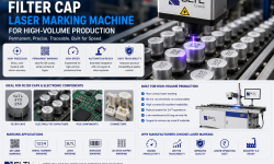
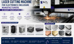
Electronics manufacturing is evolving faster than ever. Component sizes are shrinking, production speeds are increasing, and traceability requirements are becoming stricter. In this environment, the SPM laser marking machine has become a critical tool for electronics manufacturing. It supports both 2D and 3D laser marking on a wide range of components and materials. Traditional labeling and inkjet printing methods can no longer meet the demands of modern production. They wear out, fade, and fail in automated lines. Industrial automation now demands a marking solution that is permanent, contactless, and fast. That solution is laser marking — and the SPM series delivers exactly that.
Why SPM Laser Marking Machine Is Important for Electronics Manufacturing
Modern electronics components are smaller, denser, and more complex than ever before. Every PCB, semiconductor, connector, and IC package must carry a unique identifier. Manufacturers need serial numbers, barcodes, QR codes, and data matrix codes to track each component across the production lifecycle.
Traditional methods like inkjet printing or pad printing create real limitations. They use consumable inks that add operational costs. Moreover, they produce markings that fade under heat, chemicals, or abrasion. Additionally, they struggle with curved or irregular surfaces — a common challenge in 3D electronics jobs.
The SPM laser marking machine solves all of these problems. It delivers permanent, high-contrast marks without touching the component surface. Furthermore, it operates at high speeds compatible with automated production lines. Because it uses a focused laser beam, it achieves micro-marking precision that conventional systems simply cannot match.
Miniaturization is another major driver. As components shrink, the marking area becomes smaller. Therefore, manufacturers need a system that can place readable marks in extremely tight spaces. The SPM series handles this with ease — making it an essential tool in smart electronics manufacturing today.
Benefits of Using SPM Laser Marking Machine for 2D and 3D Electronics Jobs
The SPM laser marking machine offers a wide range of benefits that directly improve production quality and efficiency.
Contactless Marking Process The laser never touches the component surface. Consequently, there is zero risk of mechanical damage to delicate parts. This is especially important for fragile PCBs and thin semiconductor wafers.
High-Speed Operation SPM systems mark components at production-line speeds. Moreover, they integrate easily with conveyors and robotic handlers — supporting fully automated electronics assembly.
Precision Micro Marking The focused laser beam marks areas as small as a few microns. Therefore, manufacturers can mark extremely small components without quality loss. This is critical for semiconductor and IC package applications.
Permanent and Durable Markings Laser marks are chemically and physically permanent. They resist heat, solvents, abrasion, and UV exposure. Additionally, they remain readable throughout the entire product lifecycle — including in harsh environments.
QR Code, Barcode, and Data Matrix Marking SPM systems mark all standard code formats in a single pass. Furthermore, they support UID and 2D matrix codes required for aerospace, defense, and automotive electronics traceability.
Reduced Consumable Costs Because laser marking uses no inks, solvents, or labels, operational costs drop significantly. Additionally, maintenance requirements are minimal compared to inkjet or pad printing systems.
Industry 4.0 Integration SPM laser marking machines connect directly to MES and ERP systems. Consequently, they enable real-time production tracking and full smart factory integration. This makes them the ideal choice for modern Industry 4.0 electronics facilities.
How Laser Marking Improves PCB and Electronics Component Traceability
Traceability is no longer optional in electronics manufacturing. Regulations, customer requirements, and quality standards all demand full component identification throughout the supply chain. The SPM laser marking machine supports every traceability requirement with high precision and speed.
PCB Traceability Marking
PCBs require serial numbers, revision codes, and batch identifiers. Laser marking applies these directly onto the board surface — on bare FR4, copper layers, or solder mask. Moreover, the marks survive soldering, washing, and assembly processes without degradation.
QR Code and Data Matrix Marking
2D codes store large amounts of data in a small space. Therefore, they are ideal for compact electronics components. SPM systems mark QR codes and data matrix codes with enough resolution for reliable scanning — even on surfaces as small as 5mm × 5mm.
Anti-Counterfeit and Authentication Marking
Counterfeit electronics are a growing global problem. Consequently, manufacturers use laser-engraved micro marks and hidden authentication codes to protect their products. SPM systems support covert marking techniques that are nearly impossible to replicate.
Compatible Materials
SPM laser marking machines work across all major electronics materials:
- Plastics and technical polymers — connector housings, sensor enclosures
- Aluminum — heatsinks, enclosures, structural parts
- Copper — busbars, connectors, coils
- Stainless steel — industrial electronics housings
- Coated metals — anodized, painted, or plated surfaces
- IC packages and ceramic substrates — semiconductor components
Industries and Applications
Laser marking for traceability applies across multiple electronics sectors:
- PCB manufacturers — serial and revision marking
- Semiconductor component makers — die and package marking
- EV electronics manufacturers — battery management and inverter components
- Consumer electronics assemblers — product authentication
- EMS companies — batch and lot traceability
- Sensor and connector manufacturers — UID and compliance marking
Applications of 2D and 3D Laser Marking in Electronics Industry
The SPM laser marking machine handles both flat (2D) and curved or stepped (3D) surfaces — making it highly versatile across electronics production lines.
2D Laser Marking Applications
2D laser marking applies to flat surfaces like PCB panels, IC packages, flat cable connectors, and thin-film components. It is fast, repeatable, and ideal for high-volume batch production. For example, a PCB panel with 50 boards can be fully marked in a single automated pass.
3D Laser Marking Applications
3D laser marking addresses the growing need to mark non-flat components. Connector bodies, sensor housings, battery modules, and curved EV electronics parts all require marking on irregular surfaces. SPM 3D laser systems use dynamic focus control to maintain consistent marking quality across all surface geometries. Consequently, manufacturers achieve uniform, readable marks regardless of component shape.
Integration into Electronics Production Lines
SPM laser marking machines integrate directly with pick-and-place machines, conveyor systems, and robotic handlers. Therefore, they support fully automated inline marking without manual intervention. This is particularly important for high-volume electronics assembly and EMS production environments.
Laser marking also complements other industrial processes — including laser cutting for PCB singulation and laser welding for battery cell assembly. Together, these technologies support a complete, smart electronics production workflow.
Smart Manufacturing with SPM Laser Marking Machine
Industry 4.0 is transforming electronics manufacturing. Smart factories require systems that communicate, adapt, and report in real time. The SPM laser marking machine is built for this environment.
SPM systems connect to factory networks via standard industrial protocols. They exchange data with MES, ERP, and SCADA platforms. Therefore, every marking event is logged with timestamp, batch ID, and operator data — creating a complete digital audit trail.
Furthermore, SPM machines support remote monitoring and diagnostics. Production teams can track laser performance, adjust parameters, and detect faults without halting the line. This reduces unplanned downtime and improves overall equipment effectiveness (OEE).
Smart factory integration also means automatic job changeover. When a new product enters the line, the SPM system loads the correct marking template automatically. Consequently, changeover time drops to seconds — supporting high-mix, low-volume electronics production models.
SLTL Laser Solutions for Electronics Manufacturing
SLTL Group offers a complete range of industrial laser systems designed for electronics manufacturing. Each system addresses specific production requirements.
SPM Series — Precision 2D and 3D Laser Marking
The SPM series is SLTL’s flagship marking platform for electronics manufacturers. It delivers high-precision laser marking on both flat and 3D components. Key features include:
- Fast processing speeds compatible with automated production lines
- Dynamic 3D focus control for curved and stepped surfaces
- Compact footprint for easy integration into existing lines
- Smart automation-ready architecture for Industry 4.0 environments
- Support for all standard marking formats — serial numbers, QR codes, barcodes, UID
Fibre Laser Marking Systems
SLTL fibre laser systems deliver permanent metal marking for the most demanding electronics applications. They are ideal for:
- PCB metal layer and pad marking
- Connector and terminal block identification
- High-speed batch production of metal components
- Automotive and EV electronics component marking
UV Laser Marking Machines
UV laser systems use a cold marking process — making them the right choice for heat-sensitive electronics. They are particularly effective for:
- Semiconductor die and package marking
- Precision micro marking on thin-film components
- Plastic marking without discoloration or surface damage
- Medical electronics and sensor component marking
CO2 Laser Marking Systems
CO2 lasers excel on non-metallic materials. They are widely used for:
- Plastic housing and connector marking
- Cable and wire identification
- Packaging and label marking for electronics products
- Polymer-based insulator and gasket marking
Together, these SLTL laser solutions cover every electronics marking application — from PCB traceability to micro-component identification to smart factory automation.
Upgrade Your Electronics Production with SLTL Laser Technology
Electronics manufacturing is entering a new era. Precision, traceability, and automation are no longer advantages — they are requirements. SLTL laser systems give electronics manufacturers the tools they need to compete and grow.
Choose SLTL for:
- High-speed 2D and 3D laser marking for all electronics applications
- Permanent, durable markings that survive harsh production environments
- Full Industry 4.0 integration with MES and ERP connectivity
- Reduced consumable costs and minimal maintenance requirements
- Complete traceability from PCB to finished product
- Expert application support and after-sales service
SLTL also offers:
- Laser Cutting Systems — for PCB singulation, metal cutting, and precision part fabrication
- Laser Welding Solutions — for battery cell joining, connector welding, and precision assembly
Conclusion
Electronics manufacturing demands precision, speed, and traceability at every stage of production. The SPM laser marking machine delivers all three — supporting 2D and 3D laser marking across a wide range of components, materials, and production environments. From PCB serial number marking to semiconductor micro-marking to smart factory automation, SPM systems address the real challenges that electronics manufacturers face today. As components shrink and production speeds increase, laser marking will only become more critical. SLTL’s SPM series gives manufacturers the technology they need to meet those demands — now and in the future.
Frequently Asked Questions (FAQs)
Q1: What materials can an SPM laser marking machine mark in electronics manufacturing? SPM laser marking machines work on a wide range of electronics materials — including FR4 PCBs, aluminum, copper, stainless steel, technical plastics, coated metals, IC packages, and ceramic substrates. The correct laser type (fibre, UV, or CO2) is selected based on material requirements.
Q2: How fast does the SPM laser marking machine operate for PCB production? SPM systems operate at high speeds suitable for automated production lines. Marking speed depends on the code size and complexity, but typical QR code marking on a PCB takes less than one second per board — making it compatible with high-volume electronics assembly.
Q3: Can the SPM laser marking machine handle 3D curved electronics components? Yes. SPM 3D laser marking systems use dynamic focus control to mark curved, stepped, and irregular surfaces with consistent quality. This makes them ideal for connector bodies, sensor housings, battery modules, and other non-flat electronics parts.
Q4: Does the SPM laser marking machine integrate with Industry 4.0 smart factory systems? Yes. SPM machines connect to MES, ERP, and SCADA systems via standard industrial protocols. They support real-time data logging, remote monitoring, and automatic job changeover — making them fully compatible with smart factory and Industry 4.0 production environments.
Q5: What maintenance does an SPM laser marking machine require? SPM laser marking machines require minimal maintenance compared to inkjet or pad printing systems. There are no consumables to replace. Routine checks include optics cleaning, cooling system inspection, and software updates. SLTL provides full after-sales support and preventive maintenance programs.